
Research-VLSI Circuit Design
VLSI Circuit Design
CADENCE circuit design tool is used for implementation of firing CMUT circuity. Figure 1 shows an example of firing circuit block diagram. Each array in the firing circuit has 8 bit register, 8 bit multiplexer, one shot circuit , pulse generation circuit and inverter. FPGA board supports the control input signals to the firing circuitry. Figure 2 shows the transistor level implementation of each block.
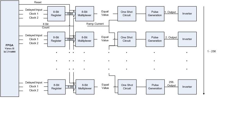
Figure 1. Block Diagram of Firing Circuit
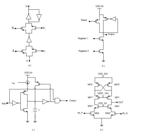
Figure 2. a) Implementation of shift register circuit, b) Implementation of one shot circuit, c) Implementation of multiplexer circuit, d) Implementation of pulse generation circuit